The semiconductor industry thrives on predictability, but its future may be shaped by technologies once considered peripheral. With EUV nearing physical and economic limits, innovation is no longer confined to shrinking transistors. Instead, next-generation fabs are expanding the scope of what counts as viable scaling. Erik Hosler, a strategic voice in lithographic research and cross-disciplinary innovation, points to a developing landscape where MEMS, MOEMS, and quantum effects are becoming legitimate candidates for redefining the roadmap.
The SPIE Advanced Lithography conference made one thing clear: the definition of “advanced” is changing. Foundries are no longer just upgrading scanners or refining resists but are exploring technologies that operate beyond the conventional toolkit. In this new context, miniaturized mechanical systems and quantum-based measurement techniques are no longer niche but increasingly foundational. This shift isn’t a departure from Moore’s Law as much as a reinterpretation of what technological progress looks like.
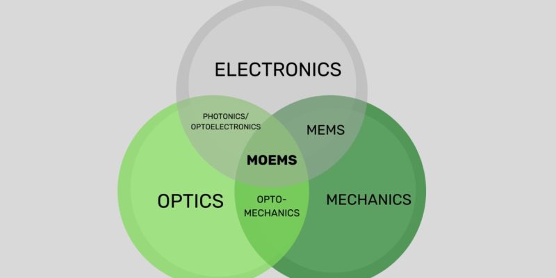
MEMS and MOEMS Enter the Litho Conversation
Micro-electromechanical Systems (MEMS) and their optical counterparts, Micro-Opto-Electro-Mechanical Systems (MOEMS), have traditionally served applications in sensing, projection, and precision actuation. In recent years, however, their relevance to semiconductor manufacturing has grown. These miniature systems can add dynamic adaptability to lithographic platforms, offering real-time calibration, active alignment, and even in-situ monitoring.
In patterning, MOEMS technologies are being explored for adaptive optics, enabling on-the-fly adjustments to correct for aberrations or drift. MEMS components embedded within mask aligners or wafer stages can introduce motion precision previously unavailable at the nanoscale. The result: patterning systems that are not only more accurate but also more robust in the face of environmental variation.
These benefits are critical as the industry grapples with stochastic defects, increasingly sensitive resists, and tight overlay tolerances. While EUV and High-NA systems push the boundaries of optics, MEMS and MOEMS can supply the mechanical agility to keep everything coordinated.
MEMS devices’ modularity makes them well-suited for scalable upgrades. A fab could retrofit existing tools with MEMS subsystems to enable higher performance without a complete equipment overhaul. That modular advantage aligns with the industry’s need for incremental improvements amid rising capital costs.
Quantum-Enabled Insights in the Fab
Quantum technologies are often associated with computing or encryption, but their implications for semiconductor manufacturing are equally compelling. At SPIE, researchers emphasized quantum metrology as a breakthrough area, particularly in understanding the photon-material interactions that define modern lithography.
Photon entanglement, tunneling effects, and other quantum phenomena are being studied to improve measurement precision. These techniques could reveal subatomic variations in resist behavior, offer real-time diagnostics of stochastic effects, or support the next generation of in-line metrology tools.
Erik Hosler says, “Last year, we included MEMS and MOEMS, and we will keep expanding to quantum to make this a place to ask questions … Lots of great things are going on, and something will emerge.” His comment underscores the mindset driving this new exploratory phase. Rather than assume any one technology will win out, the industry is building a forum for experimentation, where emerging fields can cross-pollinate with traditional process engineering.
This approach opens new doors. For instance, quantum sensors might one day provide sub-picometer measurement resolution, enabling fabs to see and correct flaws long before they affect yield. Combined with MEMS-based actuation and MOEMS-driven alignment, the fab of the future could be a hybrid of classical and quantum control.
Quantum-inspired algorithms are also being considered for layout optimization, helping to solve complex design problems that classical computing struggles with. These approaches may eventually be used to fine-tune multi-variable lithographic parameters or automate error correction protocols at the wafer level.
Integration Challenges and Opportunities
Integrating MEMS, MOEMS, and quantum elements into semiconductor fabrication is not without hurdles. These technologies often come with unique environmental or packaging requirements. MEMS devices can be sensitive to contamination or mechanical stress, while quantum systems may require temperature stabilization or vacuum enclosures.
To make them viable for high-volume manufacturing, fab designers must rethink tool architecture, system interfaces, and control schemes. In many cases, success will depend on how well these new elements can be modularized and embedded into existing workflows.
Fortunately, early case studies offer promising results. At a recent workshop, a prototype MOEMS alignment system demonstrated a 40% improvement in overlay accuracy for multilayer patterning. Similarly, quantum-enhanced sensing tools have started showing potential for detecting nano-defects invisible to current inspection systems.
The payoff is significant. MEMS-actuated litho stages can compensate for tool variation in real time. Quantum metrology platforms can enhance process windows by delivering deeper insight into variability sources. MOEMS components might even support the creation of reconfigurable exposure systems that adjust dynamically based on layer complexity.
Rethinking the Role of Foundries
Foundries have long been seen as execution centers, places where R&D ideas are brought into mass production. But the emergence of cross-disciplinary tech is changing that narrative. The fab is now a testbed, an innovation platform in its own right.
This change repositions foundries as active participants in research collaboration. More fabs are partnering directly with universities, national labs, and startups to prototype, test, and scale novel ideas. It’s a feedback loop where production constraints drive innovation, and emerging technologies reshape what production looks like.
To that end, several leading-edge foundries have launched dedicated innovation hubs. These centers allow rapid prototyping of MEMS-integrated tooling, quantum-sensing modules, and adaptive MOEMS control platforms. By accelerating iteration cycles, they reduce the time between lab discovery and production deployment.
Fabs willing to embrace MEMS, MOEMS, and quantum tools will be better positioned to extend and redefine Moore’s Law. As device functionality grows increasingly heterogeneous, scaling is becoming as much about integration as it is about size reduction.
A Flexible Roadmap Forward
What comes next may not follow the traditional node-based progression. Instead, the roadmap may splinter into branches that reflect functional innovation as much as dimensional achievement. Some paths will lead through deeper software integration, others through optics and mechanics, and still others through quantum science.
In this future, flexibility will be the most valuable currency. Foundries that build flexible infrastructure able to support new materials, new tool architectures, and new metrology regimes will lead the next chapter in chip manufacturing.
The inclusion of MEMS, MOEMS, and quantum systems is not a detour. It’s an expansion. One that redefines the fab not as a static endpoint but as a living, developing system. And that, more than any single breakthrough, is what may ensure the industry continues to thrive in the years ahead.
This development is already shaping industry culture. Engineers from traditionally separate domains are collaborating more closely, and technical conferences are fostering interdisciplinary sessions where lithographers sit beside quantum physicists and MEMS designers. The silos are slowly coming down, and the fab is emerging as a truly convergent ecosystem.
In the years to come, the success of advanced manufacturing will depend not only on who builds the smallest transistor but also on who adapts most intelligently to a changing field of tools and technologies. The future of the Fab is not fixed. It is being written in real time by the very minds willing to expand the definition of what is possible.